
Understanding Printed Circuit Boards (PCBs)
Guides
Mục Lục
What is a Printed Circuit Board?
Anyone who has ever opened up a piece of electronic equipment has seen a printed circuit board, also known as a PCB. They are thin, flat, and often green rectangular substrates that are covered with a maze of fine copper lines and silver pads and are the heart and soul of most electronic equipment. Understanding circuit boards requires learning about what they are, the different types of circuit boards that exist, the components used on these circuit boards, and the PCB Manufacturing methods or processes. A starting point is to understand how printed circuit boards evolved.
Printed circuit boards replaced point-to-point construction in most electronics during the 1950s. Point-to-point construction used wires soldered to terminal strips, boards stamped with metal loops. In a point-to-point operated device, small electronic components and their wires were directly soldered to the terminals, as were the wires from the larger devices, such as transformers. As you might imagine, this system involved a confusing tangle of wires. It was also difficult to use in mass production since each wire and part had to be looped and soldered to the correct part on the terminal strip.
Another method of circuit board manufacturing popular in the 1960s was wire wrap. Electronic components were mounted on an insulating board and interconnected by wire, with wire wrapping several times around leads or socket pins.
Enter the PCB, which did away with almost all of the wiring used in point-to-point construction and wire wrapping and in doing so, facilitated mass production. The PCB manufacturing process can be largely automated, decreasing the risk of engineering flaws that could lead to failed prototypes or faulty boards. A PCB manufacturer can input the specifications into software that runs extensive design checks to ensure the board’s optimal performance before it is even fabricated. Automated production also means lower costs than other construction methods.
This article looks at the types of printed circuit boards, the components used on the boards, the different PCB manufacturing methods, and considerations for PCB fabrication.
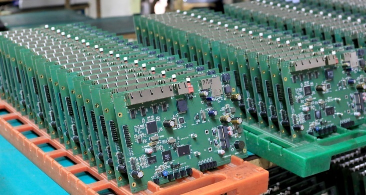
Mass-produced printed circuit boards.
Image credit: DMSU/Shutterstock.com
Types of PCBs
There are several types of circuit boards in use today. Printed circuit boards may be characterized by their construction methodology, which includes single-sided, double-sided, and multilayer board configurations.
Single-Sided PCBs
Single-sided PCBs have only one layer of substrate. The substrate is covered with a thin layer of metal on one side. Generally, copper is used because of its high electrical conductivity. This layer creates a conductive path for power and signals between various electronic components. A protective solder mask layer comes next, and a silkscreen coating may be added as a final layer to label the parts of the board. Single-sided PCBs are used for simple electronics and are mass-produced at a lower cost than other types of PCBs.
Double-Sided PCBs
Double-sided PCBs are much more commonly used than single-sided boards because the two sides allow for the introduction of more complex circuitry. Like single-sided PCBs, they have only one layer of substrate, but both sides are covered with conductive metal and the circuit components. Either through-hole mounting or surface mounting is then used to connect the components.
- Through-hole technology, sometimes spelled “thru-hole,” uses small wires, called leads, that go through the holes in the board to connect components. The leads are soldered on each end to the exact component or circuit. This is done either manually or with automated insertion mount machines. Through-hole mounting continues to be used for circuits that have to withstand more stress because the combination of leads running through the board and soldering creates a more secure connection. Through-hole PCBs are commonly used for military and aerospace products.
- Surface mounting doesn’t require holes to be drilled in the board. Components are mounted directly onto the PCB. This method uses smaller leads or no leads at all. Surface mount PCBs have become more popular than through-hole because the cost of handling and processing is much lower. Components can be soldered onto the board in bulk or by hand.
Multilayer PCBs
Multilayer PCBs have multiple layers of substrate, with insulating materials separating the layers. They use the same technology as double-sided PCBs, with the components on multi-layer boards being connected by either through-hole or surface mounting. Multilayer boards usually have four to 10 layers, but can have more if the product demands it. They are usually used for computers, servers, and are often used in specialized applications such as medical specifications PCBs.
Soldering Techniques
Soldering techniques can include hand soldering, which uses an iron, solder, soldering wick, and flux to heat a low-melting temperature alloy, usually a tin or lead alloy, that serves to mechanically join a component to a circuit board, while also providing an electrically conductive path between the pins or leads of the component and the circuit pads or traces on the board. Wave soldering is a bulk soldering process. A layer of flux is applied to the underside of the board, which is then slowly preheated to prevent thermal shock. The PCBs are then passed over a pan of molten solder. A pump in the pan washes the solder over the board to fuse all of the components to the board. Selective soldering is similar to wave soldering, but the flux is only applied to certain components that need to be soldered. Instead of then washing a wave of solder over the boards, a small bubble or fountain of solder is used to fuse specific components.
PCB Components
Interconnect Devices
Interconnect devices are usually used to connect one printed circuit board to another or sometimes to connect the board to an electronic device. They can also be used to connect an integrated circuit chip, a set of electronic circuits on one small flat piece (or chip), to a printed circuit board.
- Edge Connectors are used on the edge of a PCB and plug into a matching socket of a device. Edge connectors have metallic tracks on their sides, or traces, that convey electric signals from circuit traces on the PCB to the connector socket. The sockets contain a plastic box that is open on one side, and contains a varying number of pins inside, driven by the specific I/O needs of the circuit. Connectors are usually keyed and may contain tabs or notches that assure correct polarity and to guarantee that only the proper mating connector may be inserted.
- D-Connectors, also called D-subminiatures, get their name from their roughly D-shaped metal shields. They consist of two or more parallel rows of sockets or pins enclosed by a D-shaped metal shield that supports the connector and screens against electromagnetic interference. When used with a PCB, the pins are soldered directly to a printed circuit board and not to a wire. D-connectors are often mounted at a right angle to the PCB so that a cable can be plugged into the edge of the PCB assembly.
- Ribbon Cable Connectors are flat, thin cables that are made up of multiple smaller cables placed parallel to each other. This multi-cable arrangement makes it easy for an insulation displacement connector, also known as an IDC, to attach to one end with a row of sharp forked contacts. Termination is most commonly done at both ends of the ribbon cable connector, although sometimes only one end is IDC terminated.
- Rectangular Connectors are, as their name implies, rectangular in shape. They generally consist of a male header mounted on the PCB that can accommodate a female socket or housing.
- IC Sockets are used for the circumstance where an integrated circuit chip needs to be a removable part of a PCB. Usually, these chips are soldered onto the board, but for applications such as prototypes, where the chips need to be quickly removed and reprogrammed without having to unsolder and resolder connections, an IC socket is used. A few kinds of IC sockets are dual in-line sockets, turned-pin dual in-line sockets, and zero insertion force sockets.
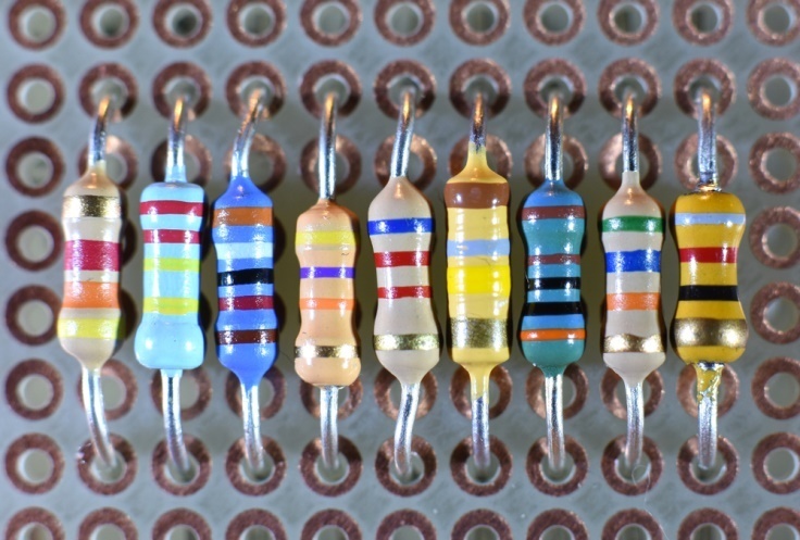
An example of resistors.
Image credit: matej_z/Shutterstock.com
Circuit Components
Printed circuit boards may be populated with a wide array of electronic and electrical components that are used to implement the desired circuit function. Broadly speaking, these devices and the resulting board designs may be classified as either analog circuits, digital circuits, or RF (Radio Frequency). The ones listed below are some of the commonly used components.
- Batteries are the basic component of any circuit. They provide a DC voltage needed for the circuit to function or to maintain power in the circuit during conditions where power supplies are not functioning. The type of battery used depends on the PCB’s application and circuit design.
- Resistors are one of the key elements of a PCB. They are small electronic devices with two terminals that can be used to regulate the flow of electric current or to produce a voltage drop. Resistors limit the flow of current and are generally color-coded with stripes to identify their resistance and tolerance levels or have their resistance value in Ohms printed on them.
- Capacitors are electronic devices which essentially store energy as an electrostatic field, and are composed of an insulating material placed between two conductive plates. In PCBs, they can block the flow of direct current while enabling the flow of alternating or time-varying current. When DC voltage is applied to a capacitor, the electric charge is stored by each conductive plate. Current flows while the capacitor is storing energy—when the capacitor is fully charged, current stops flowing. The type of material used as the insulating material (a dielectric material) determines the capacitor type. Common insulator materials include ceramic, polycarbonate and silver mica. In PCBs, the board itself often creates a capacitor, with alternating layers of metal conductive areas, a ground conductor and a power conductor, creating a stable capacitor. Within PCBs, decoupling capacitors can be found, which serve to reduce or filter noise and provide isolation by routing such noise through the capacitor or shunting it to ground.
- Diodes are electrical devices that only transmit current in one direction, and are comprised of semiconductor material between two terminals (a p-type and n-type semiconductor material on each end). While enabling current in one direction, diodes block current in the opposing direction. LEDs are light-emitting diodes. They generate visible light when an electrical current flows through them.
- Transistors are semiconductor devices that can amplify or switch the current. Transistors have three terminals that connect to the circuit. The current applied to one pair of the terminals controls the way the current runs through the other pair of terminals, either switching its direction or amplifying it.
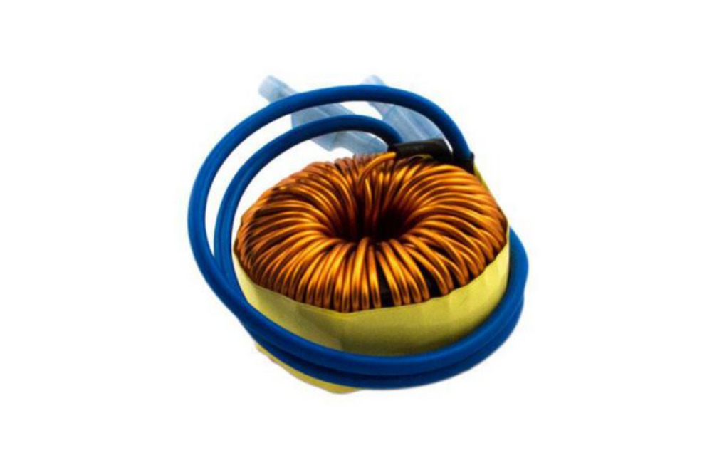
An example of an inductor.
Image credit: MPS Industries
- Inductors, also called coils, chokes, or reactors, consist of a coil of wire, usually wrapped around a ferromagnetic material core. The current passes through the wire and creates a magnetic field that then stores energy and opposes any changes in the current. They are used to resist changes to AC currents while DC currents flow through them.
- Switches either allow the current to flow or block it, depending on if they are open or closed.
Circuit Component Packaging Styles
There are many different integrated circuit package types, and the type used depends on both the IC and the type of PCB. One of the main ways they’re differentiated is by how they’re mounted onto a PCB, by through-hole, surface-mount, or sockets. These are some of the more common types:
- Dual In-line Packages, or DIP, is the most common through-hole packaging for ICs, but can also be used with sockets. They have two parallel rows of electrical connecting pins attached to a rectangular housing.
- Single In-line Packages, or SIP, have one row of connecting pins. They aren’t as common as DIPs but are often used for RAM chips and multiple resistors with a shared pin.
- Surface-Mount Packages, or SMD/SMT packages, come in many different varieties. Three of the more popular types are small-outline IC packages, quad flat packages, and small grid arrays. Small-outline IC (SOIC) packages are like smaller DIPs with the pins bent outward. They are considered to be among the easiest to solder. Quad flat packages have IC pins splayed out on each of their four sides, and are most often used for packaging microprocessors, sensors, and other modern ICs. Ball grid arrays are intricate packages with balls of solder arranged in a grid pattern on the bottom of the IC.
PCB Manufacturing Methods
While the design and manufacture of PCBs are often outsourced, knowing the means of manufacturing may help when choosing a manufacturer. Although circuit board fabrication is an evolving process, PCB manufacturing generally relies on a set of basic techniques that includes machining, imaging, plating, etching, and laminating. Each of these methods has its own advantages and limitations, and there is some overlap in their functions.
Design
Printed circuit board assemblies are relatively inexpensive to manufacture, especially in long production runs. As you would expect, the most costly and challenging part of the PCB is not its manufacture, but the PCB design. Many factors play into the maze-work design operation that is PCB engineering. Components must be properly mapped, copper to board ratios kept even to reduce waste and prevent warping, distances between tracks and components placed to avoid cross-talk or coupling, and track widths must accord with the signal frequency and current. In other words, PCB engineering is a highly specialized function, and circuit board layout is often the most expensive aspect of PCB production. When board designs involve RF (radio frequency) components, placement becomes extremely critical as the performance of RF assemblies may be severely impacted should the devices not be placed correctly in relation to the wavelength of the signals.
Machining
The machining stages of printed circuit board manufacturing revolve around the ability to drill small holes accurately and in high volume, with diameters measured in the hundredths and thousandths of an inch. Such small sizes formerly prevented the stacking of multiple boards due to the risk of breakage or distortion of the hole walls, but current technology allows multiple stacked boards to be drilled simultaneously without damage. At a scale below approximately 0.0135-inch diameters, drill bits tend to be more expensive and less resistant to operational wear. Additionally, when the ratio of board thickness to hole diameter increases, plating reliability may be negatively impacted. Mechanical or laser drilling is generally used for hole creation, and thinner boards tend to be easier to drill down to tight tolerances. For smaller and more sensitive PCBs, the ease of precision laser cutting has made laser cut circuit boards more popular.
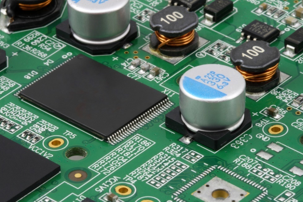
A close up of PCB components.
Image credit: Benson HE/Shutterstock.com
Imaging
Screen printing was one of the first techniques developed for circuit board imaging and has remained in use due to its low material requirements, relatively low capital investment costs, and capacity for high-volume production. However, its effectiveness decreases under smaller space and line dimensions, with specialized screens needed for working with shorter line widths and denser spacing limits. Photoimaging is a more common technique for multilayer and fine-line circuitry applications, and it involves the production of films through liquid roller coating, dip or spin coating, hot roll laminating, and electrophoresis. It is a highly accurate process for registering circuit images onto a board and is streamlined because the same tooling system is responsible for both imaging and hole-to-pin alignment. Despite its advantages, several factors can result in photoimaging flaws, including:
• Stress relaxation, which can occur in an inner layer, which causes unintended movement within a device panel and between individual panels.
• Tool wear occurs when a tooling system becomes worn from repeated use. Worn tooling can create oversized pin holes which creates loose components, threatening the circuit board’s integrity.
• Delamination cycles, where elevated temperatures and thermal cycling can increase the risk of etched features pulling up from their designated areas on the board.
• Inner-layer preparation is important because applying too much pressure during the mechanical scrubbing process can cause the laminate to stretch or distend.
• Polyester imaging films may expand or contract depending on the temperature and humidity levels of the production setting.
Steps can be taken to alleviate the risk these variables present. Micromodification, which enlarges aspects of the film to improve imaging registration, and film stretching, which extends printed images to compensate for future shrinkage, are two common methods for maintaining print accuracy. In addition, working in a clean room environment can reduce the chance of contaminants affecting the imaging quality.
Laminating
Lamination methods are used for both multilayer circuitry design and producing the actual circuit boards themselves. Hydraulic hot press lamination was one of the most common techniques originally in use, but more recently developed alternatives, such as hydraulic press variants that incorporate hot or cold processes and vacuum assistance, are employed in a wide range of applications due to their capacity for manufacturing high-layer-count boards. These methods also enable greater control over the dielectric constant and impedance of the circuit board material. Autoclave lamination offers computer-controlled accuracy and greater control over the heat levels used in the laminate resin system and is capable of producing three-dimensional forms.
Plating
PCB Plating involves the application of metal finishes to a printed circuit board, and there are several common methods for affixing metal to a board’s substrate, including:
• Electrolytic Plating is frequently used for high-volume finishing projects because it offers a relatively rapid rate of operation. The electrolytic process relies on an electric current to plate metals out of solution and typically employs a plating bath to accomplish deposition.
• Electroless Plating uses a combination of catalysts and self-reducing plating baths or galvanic cell reactions to achieve a finish without relying on an electrical power source. It is frequently used for molded circuit applications, particularly in the metallization of three-dimensional circuit paths.
• Plasma Plating, also known as dry plating, deposits metal through a partial vacuum, employing an inert gas plasma to remove metal particles from a charged target to be redeposited on a substrate. This method is commonly used in fine-line circuit production and produces relatively little waste.
Etching
Etching is the removal of excess metal from a printed circuit board surface to establish uniformity, which is critical for certain types of circuit devices, such as fine-line circuits. Standard etching methods range in capabilities from dip tanks to vertical and horizontal processes, but most techniques fit into the print-plate-etch sequence commonly found in circuit board production. Common etching chemicals include nitric acid, acid peroxide, and cupric chloride, which are limited in feature size according to copper thickness. Technologies such as additives and bonding agents may be used to reduce these limitations and enhance fine-line circuit etching.
Conformal Coating
Conformal coating is a thin film that protects the PCB components. The polymeric film follows the contours of the board to protect against dust, moisture, extreme temperatures, and other irritants. Traditional conformal coatings usually have a resin base and are semi-permeable. They’re applied in a variety of ways, including brushing, manual or automated spraying, and dipping. The coating is usually very thin so as not to add any extra weight to the PCB and to minimize heat entrapment.
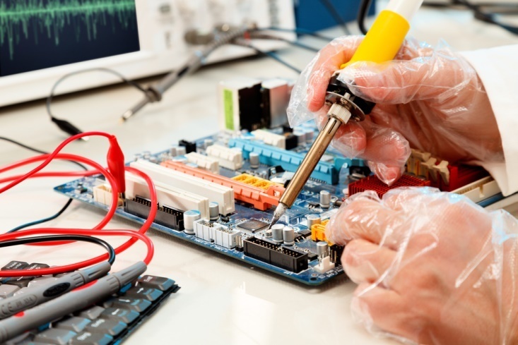
Circuit board repair.
Image credit: Science Photo/Shutterstock.com
Fabrication Considerations
Printed circuit board prototypes can be extremely helpful during the PCB manufacturing process because they provide a means of testing multiple aspects of the designed component before it is mass-produced. Finding a job shop with prototyping capabilities will help with overall PCB assembly.
When choosing a contract manufacturer for PCB fabrication and assembly, be sure that the fabrication shop can meet the turnaround time and technological expectations. Shops often specialize in one type of PCB or one type of mounting, so it’s important to find a shop that suits your production run needs.
For example, when it comes to fabricating PCBs with small dimensions, smaller drills or laser technology are required. Other PCB specialty procedures, such as depth drilling and sequential lamination, may be offered by a fabrication shop, but if specialized processes are needed, be sure to check in advance. Sequential lamination requires that boards be laminated two at a time instead of as one large batch. Depth drilling is used when holes need to be drilled to a specific depth without breaking through the other side of the circuit board. Depending on its applications, a circuit board may also require special materials, so it’s important to find a manufacturer who can acquire those materials. Flexible and rigid-flex PCBs use materials such as plastic that can bend and move, to create lighter weight and PCBs for aerospace and medical applications. Manufacturers may also specialize in a specific industry.
Summary
This article presented an understanding of printed circuit boards. For more information on related products, consult our other guides or visit the Thomas Supplier Discovery Platform to locate potential sources of supply or view details on specific products.
Sources:
Other PCBs Articles


![Toni Kroos là ai? [ sự thật về tiểu sử đầy đủ Toni Kroos ]](https://evbn.org/wp-content/uploads/New-Project-6635-1671934592.jpg)